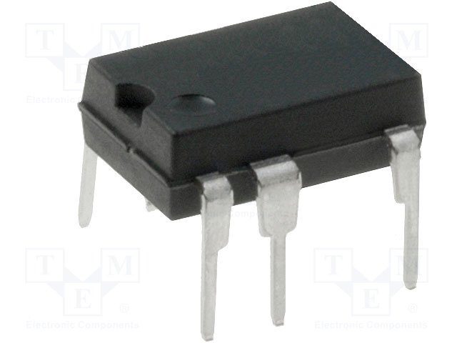
TOP253PN advanced feature set integrated switch
The most important consideration for any electrical/electronic system is power system control. This includes ensuring a reliable supply, regulating and controlling distribution, and protecting against faults and other contingencies. Therefore, designing to achieve stable, safe operation must always be a guiding principle of PCBA development.
Today, most power distribution networks (PDNs) incorporate electronics to perform the necessary monitoring and switching functions that make sure components and loads have the power they need when they need it. One device that exhibits the necessary capabilities to perform these functions for many electronic power supplies is the TOP253PN integrated off-line switcher. Implementing the advanced features of this device, which is a prerequisite for effective design and development, requires a good understanding and utilization of the TOP253PN datasheet.
TOP253PN Important Design Paramaters
The TOP253PN datasheet is the most important resource when designing a power supply control circuit with this advanced component. The datasheet is a comprehensive document and includes data and information for the TOP252-262 TOPSwitch-HX family of integrated switchers. For the TOP253PN specifically, the following design parameters are important to know.
|
TOP253PN DESIGN PARAMETERS |
|
|
Parameters |
Values |
|
Breakdown Voltage |
700 V |
|
Case/Package |
DIP |
|
Frequency |
66 kHz |
|
Height |
3.68 mm |
|
Length |
9.83 mm |
|
Max Duty Cycle |
83 % |
|
Max Input Voltage |
265 V |
|
Max Input Voltage (AC) |
265 V |
|
Max Operating Temperature |
150 °C |
|
Max Power Dissipation |
38 W |
|
Min Input Voltage |
85 V |
|
Min Input Voltage (AC) |
85 V |
|
Min Operating Temperature |
-40 °C |
|
Mount |
Through Hole |
|
Number of Outputs |
1 |
|
Number of Pins |
8 |
|
Operating Supply Current |
1.3 mA |
|
Output Current |
1.37 A |
|
Output Power |
38 W |
|
Output Voltage |
700 V |
|
Packaging |
Cut Tape |
|
Power Dissipation |
9 W |
|
Power Rating |
25 W |
|
Radiation Hardening |
No |
|
REACH SVHC |
No SVHC |
|
RoHS |
Compliant |
|
Switching Frequency |
132 kHz |
|
Topology |
Flyback |
|
Width |
6.6 mm |
The parameters above include most of the data you will need to define the functionality of the TOP253PN for your application. Additionally, it includes dimensions and specifications that must be adhered to and incorporated with your PCB layout guidelines. Prior to opting to implement the TOP253PN, it is informative to understand its architecture and features.
TOP253PN Architecture and Features
The functional block diagram from the TOP253PN datasheet is shown below. As shown, the device provides several types of control for your power supply circuit.
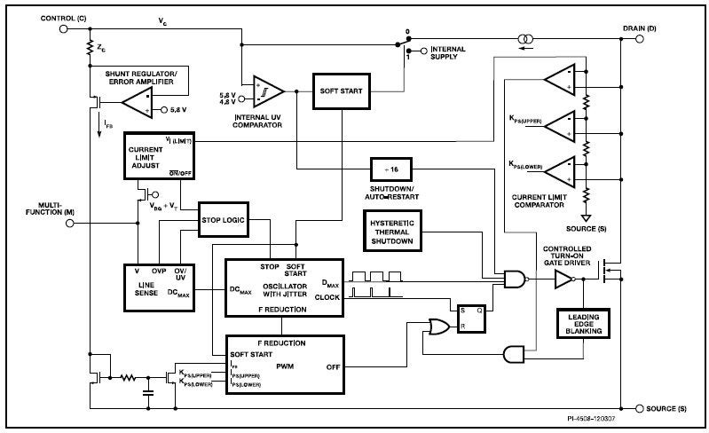
These include frequency control, under/over voltage protection, over temperature protection, remote and soft start, as well as over auto-restart. These and other features are listed below.
|
Features of the TOP253PN Integrated EcoSmart Switch
|
As this list exhibits, the TOP253PN is designed for efficient, safe, and eco-friendly operation. The variability of this component does not end with functionality. There are also several IC packaging options, which are presented in the next section, which provide you with choices to optimize your board layout.
PCBA Design With the TOP253PN Datasheet
From a connectivity perspective, the TOP253PN is not complicated. Depending upon which of the package types shown below that you select, there will be between 5 to 9 pin connections necessary.
IC Package Options
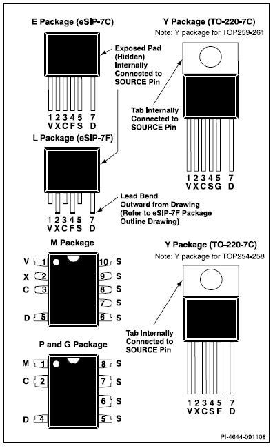
IC package options for the TOPSwitch-Hx series switches
As shown above, there are several options for component size and shape. This enables the utilization of this device in virtually any product where it’s operational capabilities can be utilized. In addition to physical structure considerations, pin connections, which are described below, are instrumental when making design layout decisions.
Pinout
|
Pin Label |
Pin Name |
Description |
|
V |
Voltage Monitor |
Over/under voltage input line |
|
X |
External Current Limit |
External current limit adjustment pin |
|
C |
Control |
Error and feedback input pin |
|
F |
Frequency |
Allows for frequency selection |
|
S |
Source |
High power MOSFET source connection |
|
D |
Drain |
High power MOSFET drain connection |
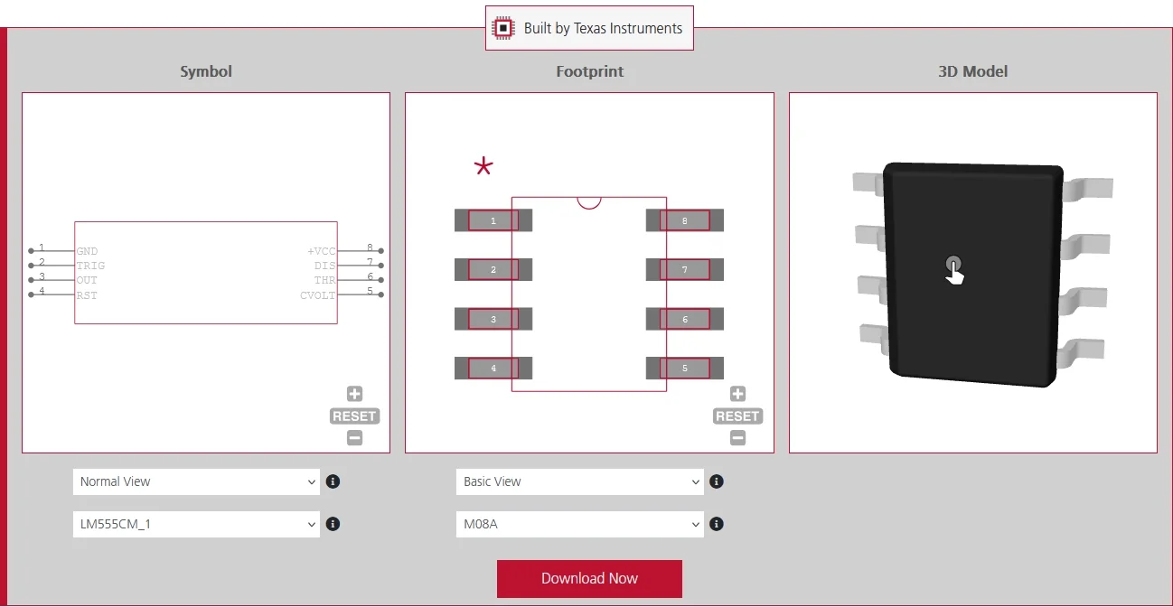
The TOP253PN may be the best solution for PDN design. For the most efficient development process when employing this advanced integrated switcher device, you should ensure that your CAD data and information is accurate and manufacturer vetted, as shown below.
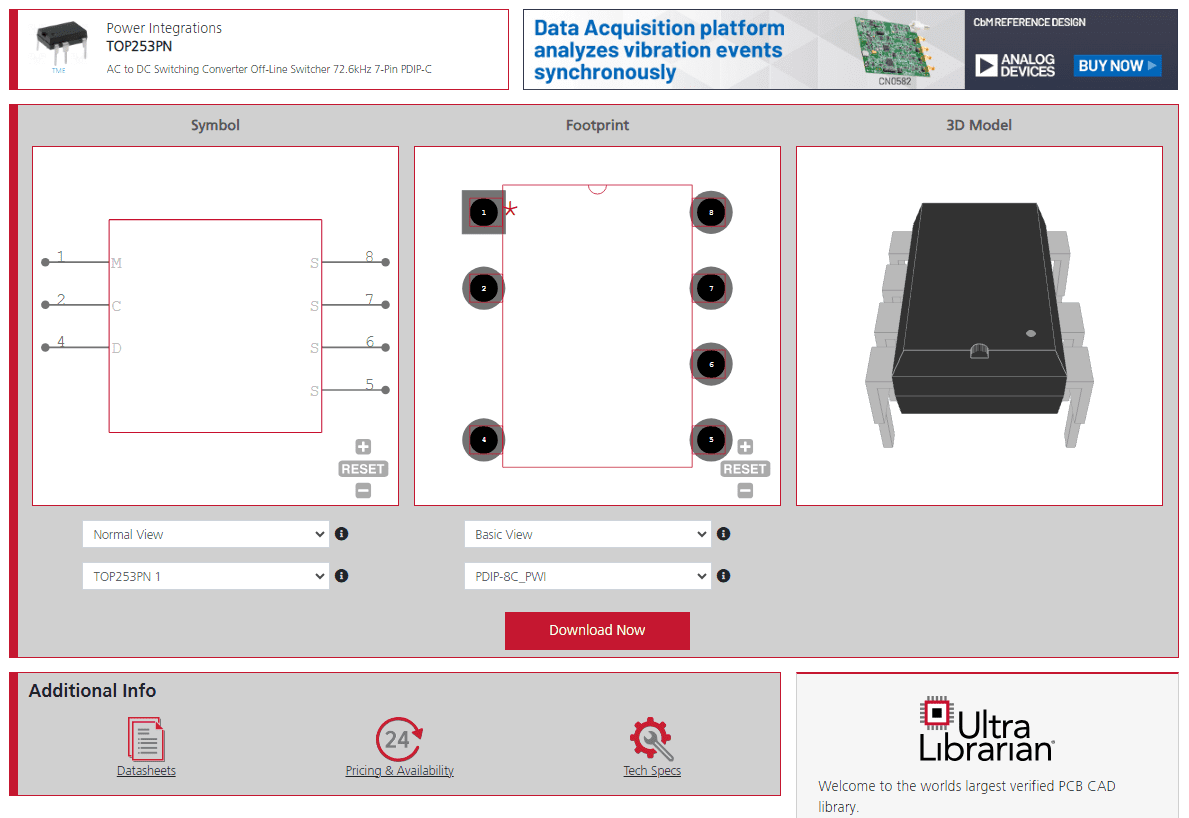
If you’re looking for CAD models for common components or important data and information like how to best use the TOP253PN datasheet for your design, Ultra Librarian helps by compiling all your sourcing and CAD information in one place.
Working with Ultra Librarian sets up your team for success to ensure streamlined and error-free design, production, and sourcing. Register today for free.
