
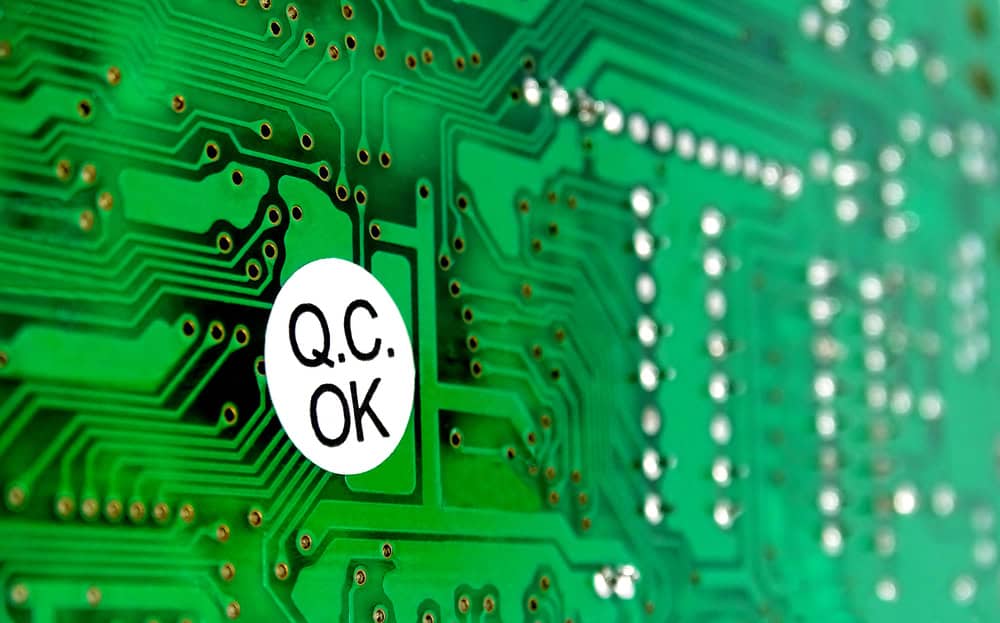
Using a good PCB verification checklist during design leads to quality certified board builds.
There is a popular saying that no job is complete until the paperwork is done. Engineers understand this as well as anyone. Yet, before the paperwork can be done, all necessary checking and testing must be done.
Evaluating an electronic circuit board often consists of two distinct but related processes: PCB verification and validation. Both of which are typically relegated to downstream development activities. For example, electrical testing to validate functionality during or after manufacturing. Failures at this point can be tremendously costly yet can be greatly mitigated or eliminated by employing a good PCB verification checklist.
Important PCB Verification Checks
Experimental validation and verification cannot–or should not–be removed from your PCB development process. However, with the right design actions and tools, the probability these testing regimens result in the need for redesign can be virtually eliminated. The key is to incorporate important PCB verification checklist considerations, as listed below, into your design.
Netlist checks, SI, PI, and thermal analyses are common design tasks, primarily instituted by performing simulations to ensure your design meets its operational objectives. DFMA, which is often performed by separate companies, is the cornerstone of the ongoing PCB manufacturing trend to integrate the intent and processes of engineers and contract manufacturers (CMs) for more efficient board fabrication and assembly. Although, perhaps underappreciated by some engineers and designers, technical cleanliness can be critical to your board’s functionality, operation and reliability.
Importance of Technical Cleanliness Checks
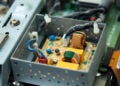
For many applications; including automotive systems, aerospace and medical devices and equipment, the standards for designing and building PCBs are very stringent. The need for this is clear: board failures can lead to serious contingencies, up to fatalities. For these critical system circuit boards, one of the most impactful hazards to reliable operation is contamination.
Technical cleanliness checks provide engineers with a means of aiding their CMs to ensure that PCBs are free from harmful debris, which is a byproduct of both fabrication and assembly processes. This and other benefits, justify the implementation of technical cleanliness verification during design.
Advantages of Technical Cleanliness Checks
- Ensure compliance with industry standards
- Verify PCB operation, performance and reliability of design
- Ensure components and boards will meet/exceed lifespan expectations
- Minimize manufacturing costs
- Improve PCB development efficiency
Obviously, incorporating technical cleanliness into your PCB verification checklist has significant positive attributes for board design and manufacturing processes. Yet, realizing these benefits requires optimizing the execution of PCB verification during design.
PCB Verification Checklist Optimization with Altair Pollex
Many PCB design software programs come with functionality that enables you to perform some of the important checks of a good PCB verification checklist. For example, leading ECAD tools allow for the importation and/or editing of constraints for design-rule checking (DRC) used to confirm DFA/DFM compliance with your CM’s rules and guidelines. Yet, most do not include the ability to perform technical cleanliness analysis.
Traditionally, the only way to perform contamination analyses was to extend the cyclic design⇒build⇒test (DBT) process to gather data from your CM–by inspection–and make subsequent adjustments to the design or manufacturing process to mitigate the impact. This is a slow and costly process that yields no usable data for design or process improvement that can be leveraged to improve development for other new product introductions (NPIs). The best solution is to incorporate a product support software tool that includes specific capabilities for technical cleanliness analyses, like Altair Pollex™.
Altair Pollex, which includes the following attributes, includes the tools necessary to help you optimize your PCB verification checklist implementation.
By employing a PCB verification checklist solution that has the attributes above, you will improve the efficiency of your design and manufacturing processes and elevate the quality of your built boards.
If you’re looking for CAD models for common components or important design information like how to optimize your PCB verification checklist, Ultra Librarian helps by compiling all your sourcing and CAD information in one place.
Working with Ultra Librarian sets up your team for success to ensure streamlined and error-free design, production, and sourcing. Register today for free.


")