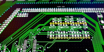
PCB component placement is the first step to realizing an assembled board.
PCB layout flows through placement. As the starting point of the layout, designers tend to race through procedural tasks like the stackup, footprints, and design rules to get to the “fun part.” Make no mistake; there is a certain gratification to deftly navigating a complex layout, but following careless PCB component placement guidelines can create a board with poor routability, ultimately affecting electrical performance.
PCB Component Placement Workflow | |
Start with critical components | Place all large components (BGAs, connectors, etc.) towards the center of the board (if mounting allows). Place any additional components with strict x- and y-positions indicated in design documents. |
Place surrounding components | “Nearby” circuitry, like resistors and capacitors that surround the central components, should be close enough to minimize impedance without restricting fanout. |
Ensure enough room for fanout | Slide or adjust the placement of the surrounding components for an unobstructed fanout. Designers may wish to create a joint object of the components for further placement planning. |
PCB Component Placement Guidelines Strategy and Tips
PCB component placement is the earliest point at which the designer can influence the performance and ease of the layout. While some designs will contain constraints for specific components or component block placement (think connectors, BGAs, etc.), most layouts rely on the designer’s experience and manufacturers’ recommendations described in datasheets. The importance of placement is difficult to understate: careful and thoughtful placement will yield a routable layout that requires minimal changes to accommodate traces/vias, but a rushed or underdeveloped placement can produce a nearly impossible-to-solve layout.
Ultimately, placement boils down to grid position: from an imaginary referenced origin, the component center will reside at some x- and y-position (this XY-data is what the pick-and-place machine receives for instruction)—as such, establishing a grid before placement is of the utmost importance. Grid placement requires a unit selection (imperial or metric), and all component placement should utilize the same units. This strategy differs from footprint creation, which may include imperial or metric units, depending on the manufacturer’s datasheet. While placing metric footprints on an imperial grid (or vice versa) can produce some rounding errors during manufacturing, these are acceptable and preferable to changing grid units to accommodate the footprint.
Some general placement instructions to follow:
- Start with large/high pinout components – These components require significant board area for component placement or signal breakout and often have multiple smaller, supporting components (pullup/down resistors, bypass capacitors, etc.) surrounding these critical components.
- Separate digital and analog – High-speed digital rise/fall times can drown out lower-frequency analog signals; separate analog and digital ground layouts promote signal integrity for the analog domain.
- Watch the clock – Due to its expansive impact, a clock signal is among the most critical signals within a design. Keep the driver/synchronizer close to the oscillator to drive down impedance and be mindful of EMI around the signal path (e.g., inductors).
- Organize components logically – Aligning components vertically and horizontally can help optimize available layout space and limit defects during installation or rework. Arranging polarized components (diodes, certain capacitors, etc.) with the silkscreen indicator pointing in the same direction can prevent reverse installation during assembly, which can damage components or the board.
- Clearance – A 40 mil/1.00 mm gap between components and a 100 mil/2.50 mm gap between components and the board edge prevents manufacturing errors and provides ample space for signal breakout/automated placement.
- Decoupling capacitors – Decoupling capacitors electrically short AC to ground for power pins, improving overall power integrity. They should reside as close to the power pin on active components as possible (while allowing signal breakout from neighboring pins).
How Assembly Impacts Placement
An essential aspect of placement is whether the assembly is single-sided or double-sided. Product managers prefer single-sided assemblies for mass-produced consumer devices to reduce excessive per-board costs. Single-sided assemblies utilize jumpers, which vias in modern design strategies have almost universally replaced. A jumper is an electrically conductive wire that lets designers cross over traces on the board. For economies of scale, the fewer jumpers (ideally zero), the more profitable the design from a manufacturing perspective.
However, many designs are unsuitable for single-sided assembly. Given the additional cost of more board layers and further board processing, double-sided assemblies can fit approximately twice as many components within the same area. To further spool out the advantage, a double-sided assembly board area can realize the same placement density of a single-sided assembly in half the board area. Designers should take care of how they distribute components between the two sides:
- Establish a primary assembly side – By default, most designers will select the top side. Large pinout components (think BGAs), connectors, or other ICs of critical circuit functionality/performance should reside on this layer. Supporting passive component placement on the opposite side of the board can be viable, but be sure signal integrity doesn’t suffer from a higher impedance pathway.
- Consider package properties – Small, low-profile SMD components can prevent heat obstruction at the bottom of the enclosure (where airflow may be less than adequate) and generate less heat overall.
- Avoid gridlock – A common strategy for double-sided assemblies is to route parallel within the plane and perpendicular to the opposite side (e.g., horizontal traces topside, vertical traces bottom side, or vice versa). This routing typically reflects a placement methodology that prioritizes “neatness” over optimal circuit blocks. While this is viable for small-scale production lots, the additional vias required to step across the perpendicular segments when routing can quickly become financially prohibitive at mass production quantities.
Ultra Librarian Gets Designers to Placement Faster
PCB component placement guidelines define a board layout’s success (or failure): a well-considered strategy provides ample board space for pin fanout and more general routing. Of course, no PCB layout can get off the ground without accurate and verified PCB footprints that ensure the assembly portion of manufacturing proceeds seamlessly. If you’re looking for PCB footprints and library management options, look no further than Ultra Librarian. With millions of verified footprints from leading vendors, you can focus on a fast, quality design turnaround time.
Working with Ultra Librarian sets up your team for success to ensure streamlined and error-free design, production, and sourcing. Register today for free.


