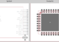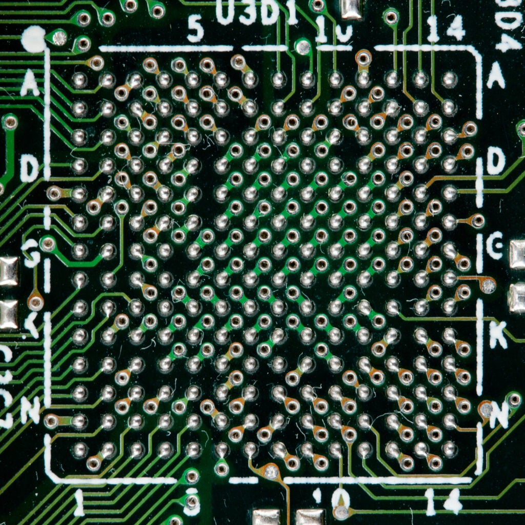
PCB footprint for a BGA component
A PCB footprint represents the exact placement and connection points for electronic components on a printed circuit board (PCB). It includes pads, which connect component pins to the PCB, silkscreen outlines for visual reference, and other markings, like polarity indicators and reference designators. The footprint ensures that each component fits accurately on the board, aligns with the correct electrical connections, and meets the manufacturing tolerances for automated assembly. This article provides PCB footprint guidelines to ensure the final circuit’s functionality, reliability, and manufacturability.
Important PCB Footprint Guidelines
An accurate PCB footprint prevents issues like misalignment, solder bridges, and open circuits that can lead to assembly failures. It ensures compatibility with automated manufacturing processes, reducing errors and streamlining production. Here are some PCB footprint guidelines for your next project.
These PCB footprint best practices ensure reliability in assembly, manufacturability, and testing while reducing errors during the PCB design and production process.
Benefits of Proper PCB Footprint Design
A properly designed PCB footprint provides several key benefits:
- Manufacturability: Well-aligned component placements and properly sized and spaced pads reduce the risk of solder bridges.
- Reliability: Accurate footprints prevent component misfits, open circuits, and short circuits. A more reliable circuit performance results in fewer chances of failure during operation.
- Assembly Process: Properly designed footprints are compatible with automated assembly processes such as pick-and-place machines and AOI, ensuring that components are placed correctly and inspected thoroughly.
- Errors and Costs: Good footprint designs minimize the chance of errors during production, such as incorrect component placement or soldering defects, saving money on reworks.
- Signal Integrity: Footprints with the correct pad sizes and clearances reduce crosstalk, electromagnetic interference, and signal reflection.
- Space Utilization: Optimizing PCB footprint design enables designers to fit more components into smaller areas while maintaining functionality.
- Consistency in Design: Having a well-established footprint library simplifies maintenance, upgrades, and collaboration among teams.
If you’re looking for CAD models for common components or important design information on PCB footprint guidelines, Ultra Librarian helps by compiling all your sourcing and CAD information in one place.
Working with Ultra Librarian sets up your team for success to ensure streamlined and error-free design, production, and sourcing. Register today for free.