
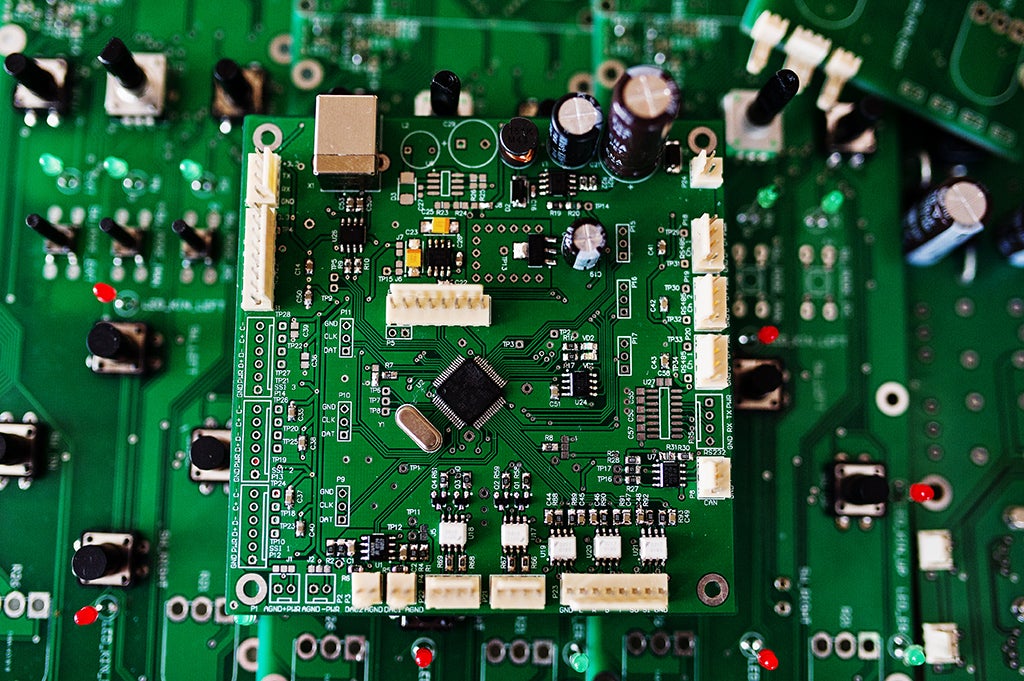
Improving engineering department efficiency produces better PCBs
The efficiency of a PCB engineering department plays a crucial role in improving product development, reducing costs, and ensuring high quality output. As electronics become more complex and time-to-market demands increase, optimizing design, prototyping, and manufacturing processes can prevent costly delays, errors, and rework. By automating processes, streamlining workflows, and setting clear goals, engineers can improve engineering efficiency, reduce bottlenecks, and produce reliable PCB designs more quickly. In turn, chip makers gain a competitive edge by improving productivity and supporting innovation.
Strategies to Improve Engineering Efficiency
Below is a table that presents the best strategies to improve engineering efficiency, from automating design processes to enhancing collaboration and monitoring performance continuously.
How to Measure Engineering Efficiency Improvement
In order to maximize engineering efficiency, you need to measure your progress once your strategies are in place. The following are common metrics to gauge engineering efficiency improvement.
Design Cycle Time
- What to Measure: Time from initial concept to final approval of the PCB design.
- Why It Matters: Shorter cycle times mean smoother processes and efficient workflows.
First Pass Yield
- What to Measure: The percentage of PCB designs that pass validation on the first try and meet all specifications.
- Why It Matters: High first pass yield means fewer iterations, lower costs, and higher design accuracy.
Defect Density
- What to Measure: Number of defects per PCB unit area.
- Why It Matters: Low defect density means high-quality designs and output.
Time to Market (TTM)
- What to Measure: Time taken from conception to market availability of the product.
- Why It Matters: Short TTM improves competitiveness and revenue potential.
Resource Utilization
- What to Measure: The efficiency of tools, equipment, and human resources.
- Why It Matters: Optimized resource utilization maximizes productivity while reducing costs.
Rework and Revision Rates
- What to Measure: The frequency of revisions or rework required as a result of errors or non-compliance with specifications.
- Why It Matters: High rework rates indicate inefficiency in design or review.
Cost Efficiency
- What to Measure: Design costs relative to budget.
- Why It Matters: Maintains quality standards while staying within budget.
Design Complexity vs. Efficiency
- What to Measure: The ratio of design complexity to time and resources required.
- Why It Matters: Shows the team’s ability to handle complex designs efficiently.
Error Discovery Time
- What to Measure: The time it takes to identify and correct design errors.
- Why It Matters: Shorter discovery times reduce downstream errors.
Adherence to Standards
- What to Measure: Compliance with industry standards and regulations.
- Why It Matters: Ensures PCB reliability, safety, and manufacturability.
A combination of quantitative metrics and qualitative factors can be used to measure engineering efficiency. Consistent, high-quality results can be ensured by regularly monitoring these metrics and implementing strategies to improve engineering efficiency.
If you’re looking for CAD models for common components or ways to improve engineering efficiency, Ultra Librarian helps by compiling all your sourcing and information in one place.
Working with Ultra Librarian sets up your team for success to ensure streamlined and error-free design, production, and sourcing. Register today for free.


