

Electronic product innovation today is based on effectively using the oldest form of communication: symbols and imagery.
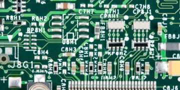
Today, it is difficult to find any product that does not directly or indirectly rely on electronics. From relatively simple functions like controlling LED indicators to driving smart devices and appliances, PCBs and the electronic components that comprise them are essential for many of the conveniences and capabilities that we often take for granted. This reliance on electronics is only going to grow as industry trends indicate new innovations in electronic components, circuit boards, and systems will continue to increase.
While the utilization and reliance on electronic technology may be relatively new, the design and building of these devices depends on effectively using one of the most basic means of communication: images. In fact, imagery is the foundational conduit that delivers necessary data and information to everyone along the path of successful PCB design and development. The first important step in this process is creating a good schematic, which is best achieved by using the correct elements and following electronic schematic symbol design best practices.
Important Electronic Schematic Symbols
Electronic schematics serve as the starting point for PCB design and development. In addition to providing the foundation for PCB layout derivation, the schematic serves as the canvas where ideas and expectations are merged with scientific principles to forge a graphical representation of a realizable product design. Active and passive components primarily comprise the schematic; however, there are other important elements, as listed below.
| IMPORTANT PCB ELECTRONIC SCHEMATIC SYMBOLS | |||
| Common Components | Other Elements | ||
| Component | Schematic Symbo | Element | Schematic Symbol |
| Resistor |  | Ground |  |
| Capacitor |  | Net |  |
| Inductor |  | Node |  |
| Diode |  | Terminal |  |
| Transistor |  | Switch |  |
| Transformer |  | Power Source | 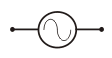 |
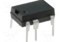
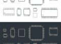
| Integrated Circuit (IC) |  | Meter | 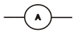 |
The listing above is not exhaustive. Many components, like capacitors, have several different symbols. These variants are typically used to indicate a specific characteristic/function for the component. The same is true for other basic electronic schematic elements. Whether the symbol is simple or complex, it must accurately convert to the circuit board footprint and include essential specifications and information for a successful PCB design and build.
Best Schematic Symbols Design Practices
Creating a schematic is both an art and a science. The artistic portion of the process is transforming an idea or set of performance criteria into a cohesive graphical representation. The science portion is selecting the best components and following the best practices, such as the electronic schematic symbols guidelines below, that make the imagery realizable.
Electronic Schematic Symbols Design Guidelines
- Prioritize accuracy in symbol selection
When selecting the best components for your design, it is important to incorporate reliability. This is achieved by sourcing symbols, footprints, and 3D models from a trusted CAD model resource.
- Use industry-standard electronic schematic symbols
To ensure that all PCB design and development stakeholders can easily read and understand the schematic, it is important to follow the rules and guidelines as set forth in well-known standards, such as IEEE/ANSI 315-1975.
- Avoid manual component CAD model creation
The greatest opportunity for electronic schematic symbol error occurs when these elements are created manually, and this practice should be avoided. A more reliable alternative is using a customized Virtual Librarian Service (VLS) where models are professionally built to your specifications and with your design intent.
- Ensure accurate simulation models and data are available
The schematic is much more than the product of the first stage of PCB design. In fact, multiple stakeholders utilize the schematic as a resource throughout the design and development workflow. Consequently, it is critical to ensure the performance and operation of the circuits through simulations like PSpice and that accurate design information is included for downstream verifications.
- Leverage component CAD model-distributor integrations
Failing to consider component shortages and other supply chain problems is planning for failure in today’s electronics industry. Aside from best practices to shore up inventory, etc., working with CAD model-distributor partners is one of the best ways to ensure your component supply chain will meet your volume requirements.
By following these best practices, you will be off to the best possible start for an efficient workflow and successful PCB design and development project.
If you’re looking for CAD models for common components or design guidelines for the most effective use of electronic schematic symbols, Ultra Librarian helps by compiling all your sourcing and CAD information in one place.
Working with Ultra Librarian sets up your team for success to ensure streamlined and error-free design, production, and sourcing. Register today for free.


