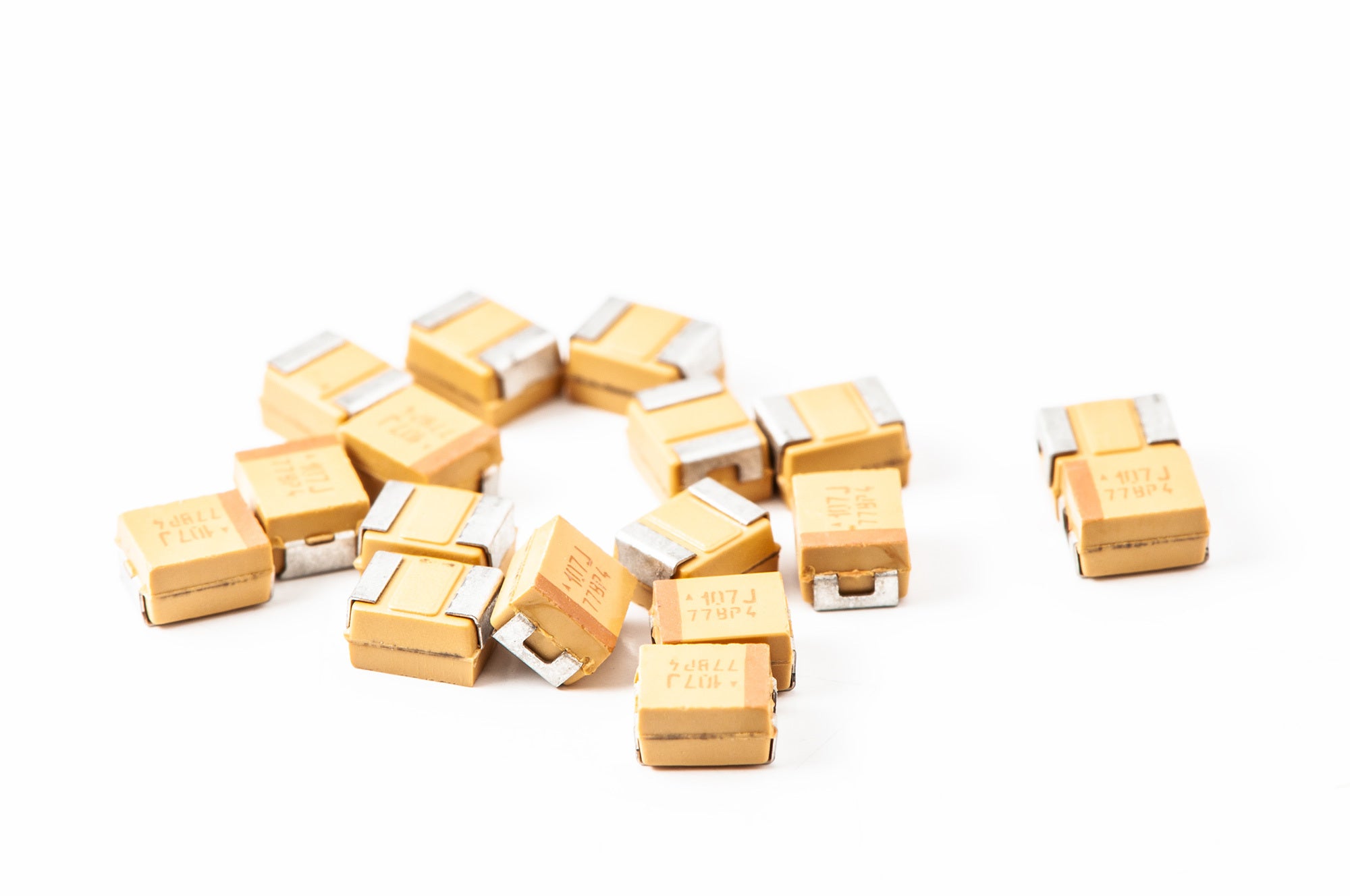
Tantalum capacitors are a good choice for PCB layout bypass capacitors.
Designers may notice the large capacitors distributed around the various ICs when designing circuit layouts or perusing schematics. These bypass capacitors supplement the primary or onboard power sources with more localized charge storage tailored to each circuit’s particular I/O needs. While some designers may not give bypass capacitors a second thought, they have many applications, as shown below, and are integral to any system’s power integrity. For PCB layout, bypass capacitor size, placement, and loading are key considerations to ensure stable performance and minimize runtime errors.
PCB LAYOUT BYPASS CAPACITOR APPLICATIONS: CURRENT VS FREQUENCY | ||
Low-frequency | High-frequency | |
Low-current |
|
|
High-current |
|
|
PCB Layout for Bypass Capacitors: Key Considerations
The bypass capacitor sources stored electrical energy whenever transient spikes occur. In layperson’s terms, think of the bypass capacitor as providing localized energy storage for nearby components. When the capacitors of an IC charge and discharge, they generate instantaneous current (i.e., displacement current) that can create ringing on the shared power net. This ringing can create false triggers or otherwise negatively impact signal integrity; bypass capacitors prevent this negative performance by sourcing low-impedance power closer to the IC.
Generally, bypass capacitors are synonymous with ceramic capacitors, as the charge density of these caps reduces adverse effects on signal integrity. However, there are other types available and other considerations, as listed below.
- Type—Capacitors are available in the following types:
- Ceramic capacitors have less storage capacity but are usually faster to charge/discharge with minimal lead impedance.
- Electrolytic capacitors have greater bulk storage but are larger, and layout designers/assemblers must ensure correct placement orientation to prevent catastrophic failure of the component. These capacitors are beneficial in low to mid-frequency bypass applications. However, their charge and discharge times are too long for rapid-switching supplies.
- Tantalum caps, like electrolytics, must be carefully placed to avoid backward installation, and are suitable for low-voltage circuits.
- Size and placement—Layout designers will want to distribute capacitors according to the time constant (which affects “total” charge/discharge time). A smaller capacitance capacitor has a shorter time constant (and vice versa). The smallest capacitance capacitors should be as close as possible to the IC’s power and ground nets, ideally connected directly to the corresponding pins with vias in the pads to further minimize impedance. Larger capacitance capacitors can be further from the power and ground pins to allow room for signal routing breakout.
- Output loading – When adding a PCB layout bypass capacitor its impact of on the load must be considered. The additional capacitance (as seen by the IC) requires more charge, which can slow down rising/falling edges. Excessive capacitive reactance on the load can exceed the bypass capacitor’s charge-sourcing ability, leading to ringing and oscillation on the power lines supplying the IC. This breakdown in power integrity can lead to systemwide logic issues (and potential damage). Smaller capacitive capacitors on the load (when possible) or additional inductance to balance the load’s reactance and make it purely resistive will prevent ringing on the power nets.
Bypass Capacitors Classification Codes
Before floorplanning/layout, it’s also worthwhile to know the values of capacitors based on an industry-standard coding system. The first letter indicates the low-temperature requirement, the first digit indicates the high-temperature requirement, and the second letter indicates the maximum deviation in stated capacitance across the temperature range (i.e., the rate at which capacitance changes as a function of temperature).
Classification of Ceramic Capacitor |
||||
First Letter | First Digit | |||
Symbol | Low-temp requirement | Symbol | High-temp requirement | |
X | + 10o C | 2 | + 45o C | |
Y | - 30o C | 4 | + 65o C | |
Z | -55o C | 5 | + 85o C | |
6 | + 105o C | |||
7 | + 125o C |
Second Letter |
|
Symbol | Max ΔC over ΔT |
A | ±1.0% |
B | ±1.5% |
C | ±2.2% |
D | ±3.3% |
E | ±4.7% |
F | ±7.5% |
P | ±10.0% |
R | ±15.0% |
S | ±22.0% |
T | ±22.0% |
U | ±22.0% |
V | ±22.0% |
Ultra Librarian Component Solutions
Before designing the PCB layout, bypass capacitor selection requires a simulation of the available packages to find the best fit between application and performance. Depending on the material and board integration (surface-mount device vs. through-hole), performance can vary wildly even for the same capacitance values; designers will want the ability to simulate and implement many different capacitors rapidly. Accessing millions of verified components for models and footprints with Ultra Librarian is easy. Moreover, getting started with Ultra Librarian is free.
Working with Ultra Librarian sets up your team for success to ensure streamlined and error-free design, production, and sourcing. Register today for free.