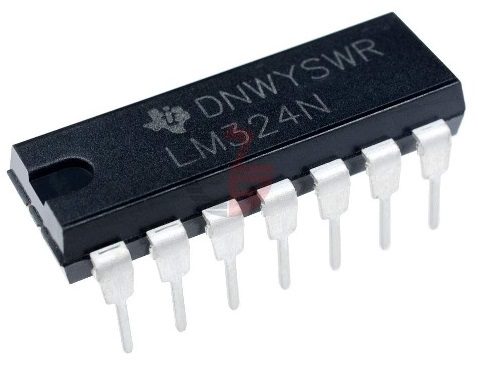
LM324N Quad Operational Amp
When designing electronic circuits, there are several component types to select an amplifier. For example, transformers can step-up or step-down voltages, currents, or powers, isolating input and output circuitry. There is also a wide range of discrete transistors used in countless applications. Then there are operational amplifiers. Op-amps have been around for a long time, and they continue to find a place in many circuit board designs. The reasons for this can be found in the LM324N datasheet.
Features and Applications of the LM324N
The LM324N exhibits some of the advantages of using operational amplifiers for your design. Not only is the component external circuitry easy to design and implement, but this package comes with four amplifiers that can be configured independently or in various stage arrangements. According to the LM324n datasheet, the amplifier allows for the use of a single source or dual power supplies, very low offset voltage and current–typically, 3 mV and 2 nA, respectively–and good PSRR and CMRR. These and other attributes support using the LM324N in the following applications.
LM324N Quad Op-Amp Applications
- Blu-ray Players and Home Theaters
- Chemical and Gas Sensors
- DVD Recorders and Players
- Digital Multimeter: Bench and Systems
- Digital Multimeter: Handhelds
- Field Transmitter: Temperature Sensors
- Motor Control: AC Induction, Brushed DC, Brushless DC, High-Voltage, Low-Voltage, Permanent Magnet, and Stepper Motor
- Oscilloscopes
- TV: LCD and Digital
- Temperature Sensors or Controllers Using Modbus
- Weigh Scales
LM324N Quad Op-Amp Parameters and Operation
In the table below, the design constraints for the LM324N are listed.
| ABSOLUTE MAXIMUM RATINGS | |||||
| Parameter | MIN | MAX | MIN | MAX | UNIT |
| Supply voltage, VCC(2) | ±13 | 26 | ±16 | 32 | V |
| Differential input voltage, VID(3) | ±26 | ±32 | V | ||
| Input voltage, VI (either input) | –0.3 | 26 | –0.3 | 32 | V |
| Duration of output short circuit (one amplifier) to ground at (or below) TA = 25°C, VCC ≤ 15 V(4) | Unlimited | Unlimited | |||
| Operating virtual junction temperature, TJ | 150 | °C | |||
| Lead temperature 1.6 mm (1/16 inch) from case for 60 seconds | 300 | °C | |||
| Storage temperature, Tstg | –65 | 150 | –65 | °C | |
As shown, the maximum supply voltage is 32V, and the differential input range is twice this value. The full range of electrical characteristics is given in the table below.
| ELECTRICAL CHARACTERISTICS | ||||||||
| PARAMETER | TEST CONDITIONS(1) | TA(2) | MIN | TYP | MAX | UNIT | ||
| VIO | Input offset voltage | VCC = 5 V to MAX, VIC = VICRmin,
VO = 1.4 V |
25°C | 3 | 7 | mV | ||
| Full range | 9 | |||||||
| IIO | Input offset current | VO = 1.4 V | 25°C | 2 | 50 | nA | ||
| Full range | 150 | |||||||
| IIB | Input bias current | VO = 1.4 V | 25°C | –20 | –250 | nA | ||
| Full range | –500 | |||||||
| VICR | Common-mode input voltage range | VCC = 5 V to MAX | 25°C | 0 to
VCC – 1.5 |
V | |||
| Full range | 0 to
VCC – 2 |
|||||||
| VOH | High-level output voltage | RL = 2 kΩ | 25°C | VCC – 1.5 | V | |||
| RL = 10 kΩ | 25°C | |||||||
| VCC = MAX | RL = 2 kΩ | Full range | 26 | |||||
| RL ≥ 10 kΩ | Full range | 27 | 28 | |||||
| VOL | Low-level output voltage | RL ≤ 10 kΩ | Full range | 5 | 20 | mV | ||
| AVD | Large-signal differential voltage amplification | VCC = 15 V, VO = 1 V to 11 V,
RL ≥ 2 kΩ |
25°C | 25 | 100 | V/mV | ||
| Full range | 15 | |||||||
| CMRR | Common-mode rejection ratio | VIC = VICRmin | 25°C | 65 | 80 | dB | ||
| kSVR | Supply-voltage rejection ratio
(ΔVCC /ΔVIO) |
25°C | 65 | 100 | dB | |||
| VO1/ VO2 | Crosstalk attenuation | f = 1 kHz to 20 kHz | 25°C | 120 | dB | |||
| IO | Output current | VCC = 15 V,
VID = 1 V, VO = 0 |
Source | 25°C | –20 | –30 | –60 | mA |
| Full range | –10 | |||||||
| VCC = 15 V,
VID = –1 V, VO = 15 V |
Sink | 25°C | 10 | 20 | ||||
| Full range | 5 | |||||||
| VID = –1 V, VO = 200 mV | 25°C | 12 | 30 | μA | ||||
| IOS | Short-circuit output current | VCC at 5 V, VO = 0,
GND at –5 V |
25°C | ±40 | ±60 | mA | ||
| ICC | Supply current (four amplifiers) | VO = 2.5 V, no load | Full range | 0.7 | 1.2 | mA | ||
| VCC = MAX, VO = 0.5 VCC,
no load |
Full range | 1.4 | 3 | |||||
LM324N Operational Architecture and Functions

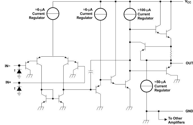
Functional block diagram of the LM324N
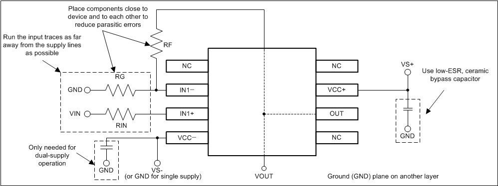
The diagram above illustrates the functional architecture of the LM324N, which comprises 115 components, including over 90 transistors. Below, a typical layout for one amplifier is shown.

LM324N implementation example
As shown, only a simple resistive network and bypass capacitor are needed to lay out the circuit–in addition to the source and ground.
PCBA Design With the LM324N Datasheet
When designing your PCB layout with the LM324N op-amp, it is important to ensure that your PCB footprint, whether manually created or from a library, agrees with your BOM entry. Due to the number of package options available, shown above, the wrong footprint can easily be used.
LM324N Package Options
| LM324N PACKAGE OPTIONS | |
| Package | Dimensions (l x w) |
| TSSOP | 5.0 mm x 4.4 mm |
| SSOP | 6.2 mm x 5.3 mm |
| SOIC | 8.65 mm x 3.91 mm |
| SO | 9.2 mm x 5.3 mm |
| CFP | 9.21 mm x 5.97 mm |
| PDIP | 19.3 mm x 6.35 mm |
| CDIP | 19.56 mm x 6.67mm |
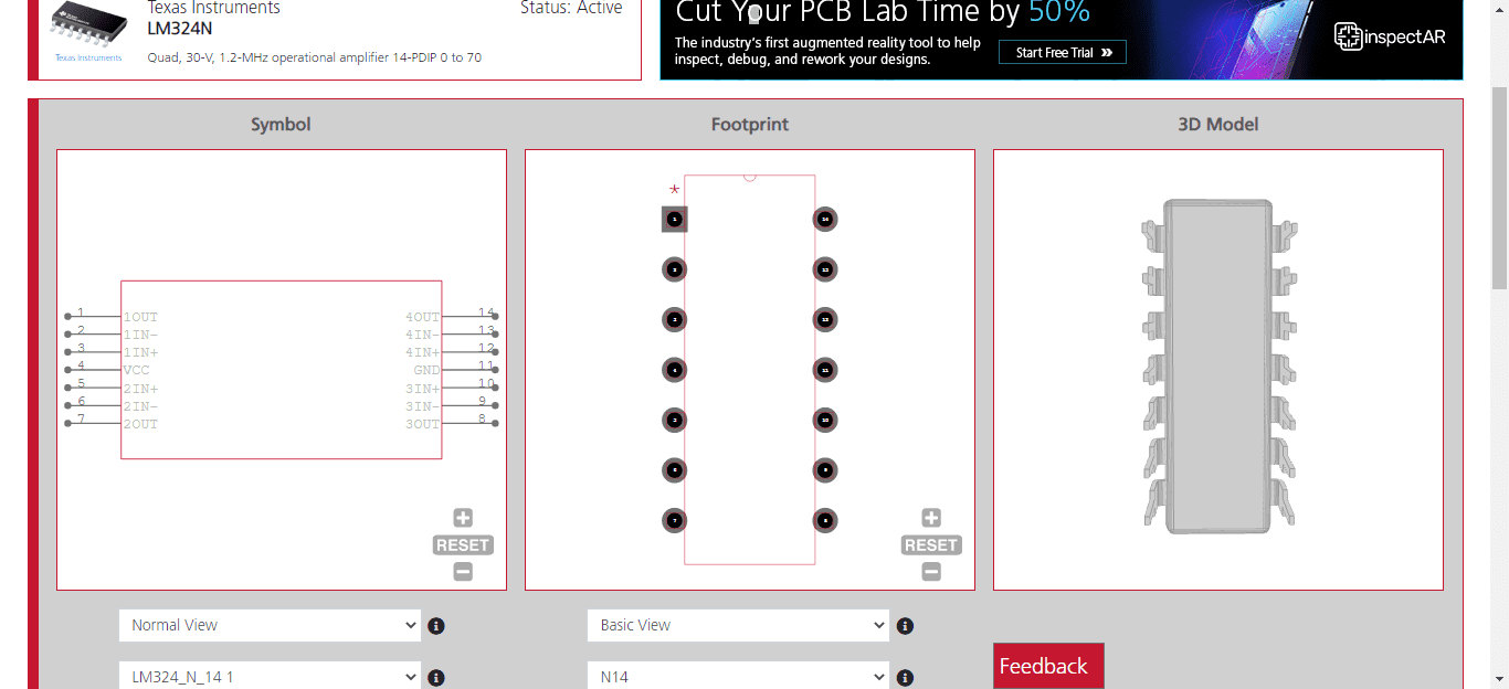
The best way to avoid this issue, which can be quite costly and time-consuming if not identified prior to submitting your design files to the CM, is to use a reliable online source for all of your component data, as shown below.

LM324N CAD data from UL
If you’re looking for CAD models for common components like the LM324N quad operational amplifier, Ultra Librarian helps by compiling all your sourcing and CAD information in one place. Working with Ultra Librarian sets up your team for success to ensure streamlined and error-free design, production, and sourcing. Register today for free.


