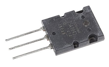
It seems so long ago that vacuum tubes were the state of technology for electrical amplifiers. Yes, they were bulky and got very hot, but they laid the groundwork for what may be possible with a smaller, more efficient, and faster switching device. That device arrived in 1947 with the invention of the transistor. In the decades that have followed, all expectations of how this invention would revolutionize the world have been shattered.
Today, transistors can be found in virtually all electronic products, and the smallest of these are in the nanometer range. However, transistors are typically used as switches and/or amplifiers irrespective of their size. In addition, in high-power applications, transistors are often substituted for relays or are used to deliver high-quality audio. A recommended component for the latter from Toshiba Electronic Devices & Storage Corporation is described in the TTC5200 datasheet.
BJT Power Amplifiers and Their Applications
Probably, the most common transistor type is the BJT. This component includes three material sections and can be constructed as either an NPN or PNP–where N denotes n-type or electrically negative, while P indicates p-type or positive. In addition, BJTs are built with three terminals: the collector, base, and emitter and three operation modes or regions, as listed below.
BJT Operation Modes
- Cutoff Region
The BJT is electrically off in this mode, and there is no current flow between the collector and emitter. This state is used as the OFF condition for a switch application. - Saturation Region
The saturation mode is effectively the opposite of cutoff. Here, maximum current flows, and the transistor appears as a short circuit. - Active Region
To be utilized as an amplifier, the BJT must be in the active region between cutoff and saturation. In this mode, an IV characteristic is established by the collector current and voltage from collector to emitter; amplification can occur along with the characteristics between the extremes of cutoff and saturation.
BJTs, such as Toshiba’s TTC5200, are well suited for high power application and/or signal transfer and fast switching.
The TTC5200 High Speed Power Amplifier
As stipulated in the TTC5200 datasheet, the TTC5200 is an NPN triple diffused BJT transistor. The component is recommended for audio applications, especially 100W output stages. And has a very high collector voltage rating of 230V along with other attractive specifications, as shown in the table below.
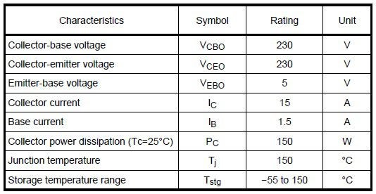
Maximum ratings for the TTC5200
The table listing includes the maximum voltages, currents, wattage, and temperatures for the operation of the TTC5200. However, these should be avoided for extensive periods; otherwise, reliability may suffer. Common electrical characteristics are given below.
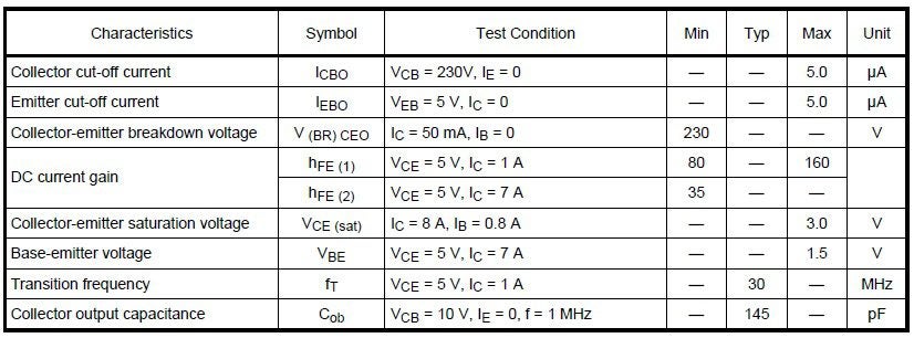
TTC5200 electrical specifications
As shown above, the transistor has a maximum DC gain of 160. This value can be approached for various collector current levels, as shown by the example IV–collector current versus collector to emitter voltage–characteristics shown in the figure below.
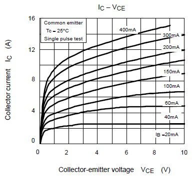
Example IV characteristics for the TTC5200
Another attractive parameter for the TTC5200 is its relatively narrow transient thermal resistance, which ranges between 0.1 < 0.9 °C/W for pulse width between 1ms and 100s, as shown in the following graph.
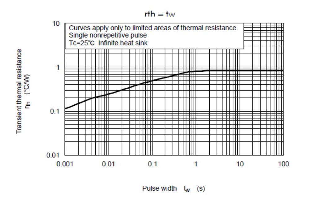
TTC5200 thermal resistance vs. pulse width characteristic
The TC5200 operation follows that of a typical BJT. Therefore, it may be necessary to perform small signal analysis before settling on the component for your application. Although not included in the TTC5200 datasheet document, a companion document contains notes on designing BJT transistors, including setting up and using T and 𝝥 models. Additionally, a PSpice model is available for advanced signal analysis, which should be performed before converting your schematic to a PCB layout.
Alternative Device
There are no plans to halt or reduce production of the TTC5200. However, Toshiba offers a similar product, the 2SC5200N, and recommends it for new PCBA designs.
PCBA Design With the TTC5200 Datasheet
The TTC5200 is available in TO-3P package format, as shown below.
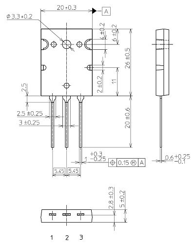
TTC5200 dimensions for manual footprint creation
This datasheet drawing is helpful to ensure accurate dimensions, whether you are creating your own component footprint or using a package template from your ECAD program’s library.
The best option for designing your new circuit board; however, is probably to rely on the TTC5200 datasheet for verifying the transistor meets your performance objectives–via signal analysis, etc.–and to utilize a comprehensive online resource that includes manufacturer verification of the symbol, footprint and 3D CAD model as shown below.
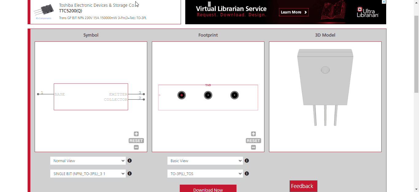
TTC5200 CAD data from UL
With this reliable data, you can be assured that the procured components will match your design file specifications to ensure manufacturability.
If you’re looking for CAD models for common components and design best practices, such as how to best use the TTC5200 datasheet for your board design, Ultra Librarian helps by compiling all your sourcing and CAD information in one place. Working with Ultra Librarian sets up your team for success to ensure streamlined and error-free design, production, and sourcing. Register today for free.



.png)


