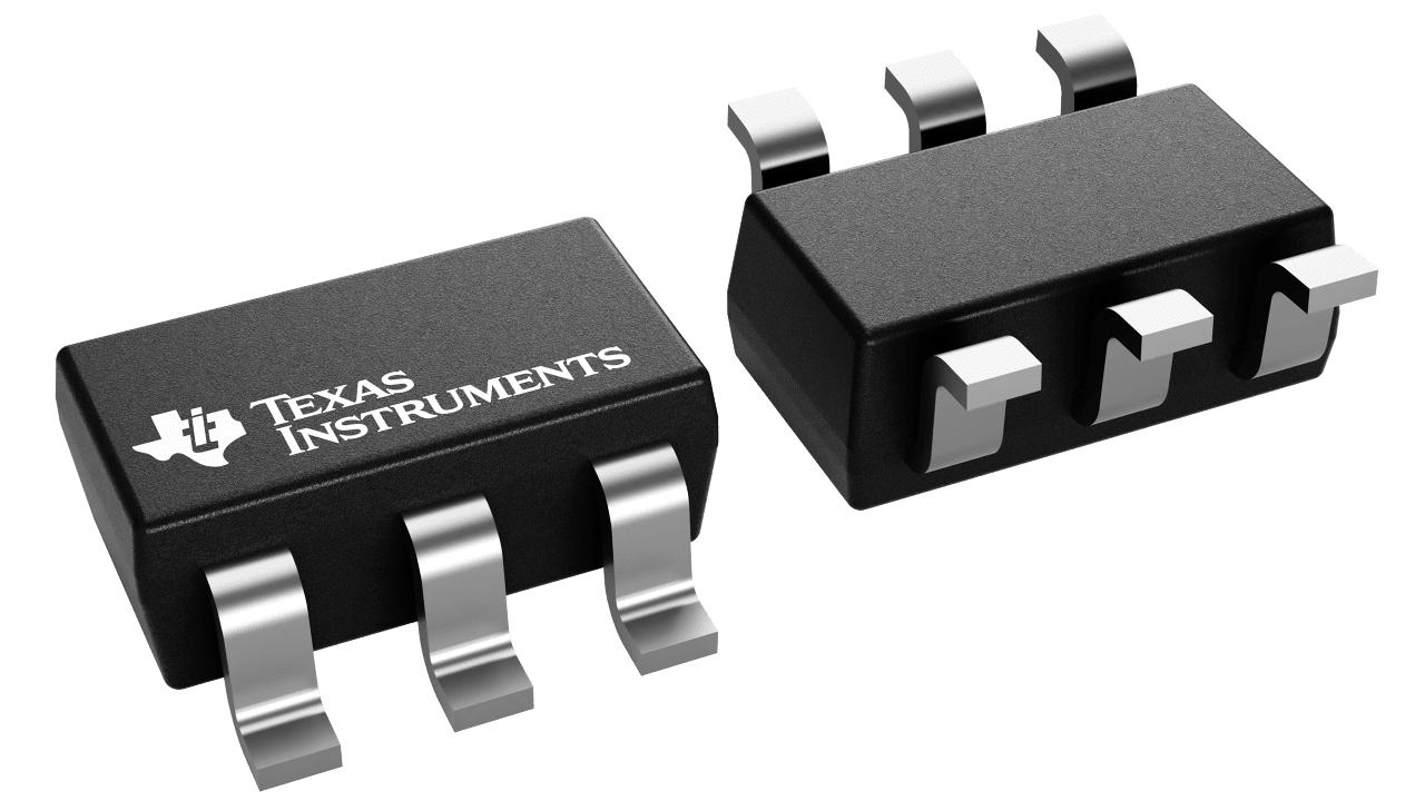
The TLV3501 is one of the highly sought-after high-speed rail-to-rail comparators that best fit automotive microsize applications. The comparator features a fast 4.5 ns propagation delay for high speed operation.
In addition, the built-in hysteresis circuit enables the device to nullify signal noise and supports further cancellation by allowing for external hysteresis circuit integration. Thus, it is an ideal bet for wireless base applications. Designers looking for its application in other areas such as DC-DC converter, HEV/EV, and hybrid power control unit should refer to the TLV3501 datasheet for more information.
Basics of a Comparator
As the name suggests, the job of a comparator is to compare two analog signals and produce a digital logical output.
It has five pins in total, as shown below.
- Two input pins – Input voltage (Vin), Reference voltage (Vref)
- One output pin- Vout
- Two power supply pins (Voltage and ground)
The block diagram is shown below.
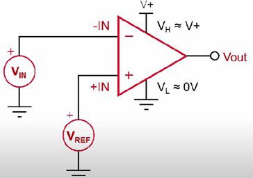
Though its schematic is similar to opamp, the functionality is widely different.
Depending on the requirement, the input voltage can either be applied to the positive terminal (non-inverting comparator) or negative terminal (inverting comparator).
The following logic table shows the operation of a non-inverting comparator.
| Vin | Vref | Vout |
| 0 | 0 | 0 |
| 0 | 1 | 0 |
| 1 | 0 | 1 |
| 1 | 1 | 0 |
For a non-inverting comparator, the output goes high when the input voltage exceeds the reference voltage, i.e., Vin>Vref, and vice versa.
Similarly, the output goes high for the inverting comparator when the input voltage is smaller than the reference voltage, i.e., Vin<Vref and vice versa.
Comparators can be broadly classified into the following two categories depending on the design of their output stage.
- Open drain comparators
- Built with bipolar transistors
- Features open collector output (LM139)
- Used for wired connections
- Push-pull comparators
- Built with field effect transistors
- Features collector-collector output
- Used for wireless connections
TLV3501 is a push-pull output comparator.
Making the Best Use of the TLV3501 Datasheet
Pin Configurations and Pin Functions
TLV3501 is available in 6-Pin SOT-23 and 8-Pin SO packages. All pin configurations and individual pin functions of both the packages are shown below.
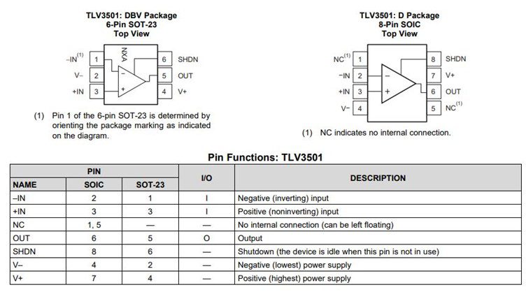
As the configurations show, the microsize packages make the TLV3501 comparator an ideal bet for portable and space-restricted wireless base applications. It has a special shutdown pin (SHDN). When the SHDN pin is not in use, the device goes idle.
TLV3501 Operation
As TLV3501 features a push-pull CMOS output stage, let’s look at its basic operation. The functional diagram below represents the internal of a push-pull comparator.
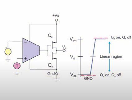
As you can see, its output is based on the output of a pair of transistors. As needed, either transistors turn on to source or sink the current to produce a high or low output.
The absolute maximum ratings of TLV3501 comparator over operating free-air temperature range has been shown below.

As per the TLV3501 datasheet, the recommended operating condition allows the TLV3501 comparator to operate between 2.2V and 5.5V, within a wide temperature range of –40°C to +125°C.
Built-in Hysteresis
Any intrinsic or extrinsic noise will affect the performance of a comparator. The output heavily fluctuates above and below the threshold point in response to the noise peaks. Thus it is highly imperative to protect comparators from such unwanted noises.
TLV3501 effectively reduces sensitivity to noise with inbuilt hysteresis. Hysteresis is a form of positive feedback to the comparator to create max upper and lower threshold levels within which the unwanted noise can be nullified with ease. These threshold levels are set according to resistors present in the voltage divider and the feedback. This is also known as the hysteresis range.
TLV3501 has a built-in hysteresis of 6mV. However, you can still improve the noise immunity by adding an external hysteresis in terms of a small amount of feedback to the positive. This is highly useful in the case of wireless base applications to stop unwanted noise from interfering with healthy signals.
High Speed Window Comparator
TLV3501 can be used as a window comparator to ensure the signal is within two required threshold ranges. As shown below, a window comparator circuit can be designed by utilizing two TLV3501 comparators in parallel.
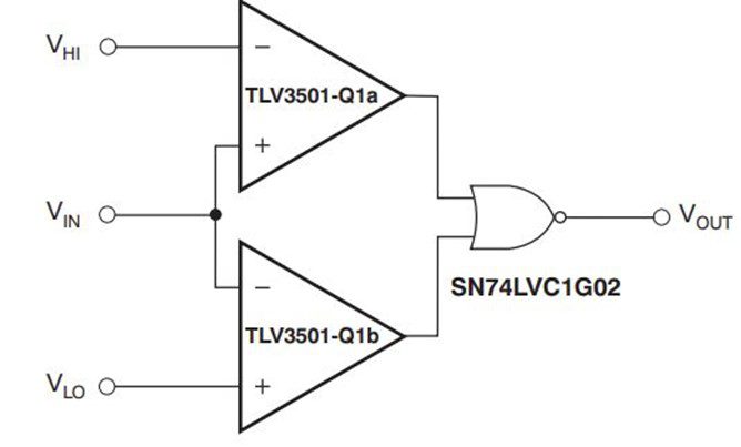
When the input signal remains within the window, the output goes high and vice versa.
Building PCBA Design with TLV3501 requires thoroughly understanding TLV3501 datasheet, footprints and sourcing data. In this regard, the Ultra Librarian gives you a complete online resource that includes PCB footprints, technical data and 3D CAD model as shown below.
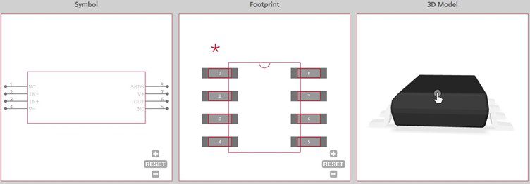
All ECAD data available on Ultra Librarian is verified by component manufacturers to help you streamline your design process. Working with Ultra Librarian sets up your team for success to ensure streamlined and error-free design, production, and sourcing. Register today for free.


