
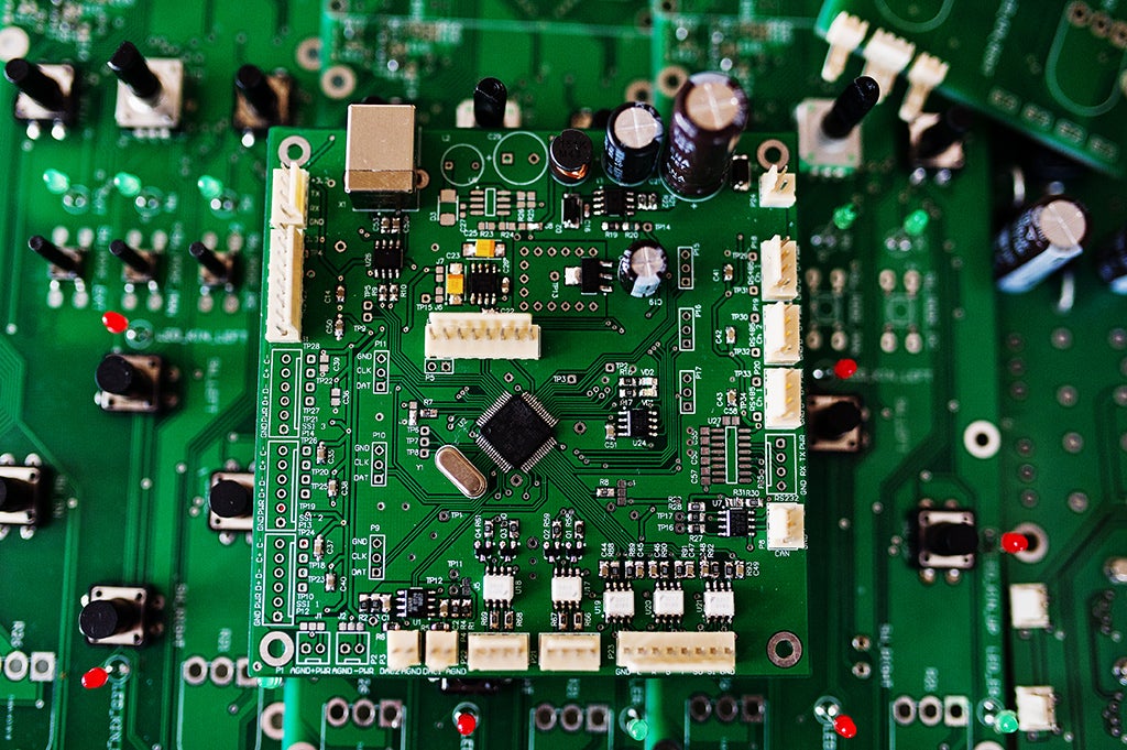
PCB component density is evershrinking, from the now rarely-used through-hole components to surface mount technology (SMT).
The drive toward miniaturization in electronics has changed how engineers approach PCB design. As consumer demand results in smaller, more powerful devices, engineers must increasingly fit complex functionality into shrinking spaces. This pursuit has created advancements in PCB component density through innovative design methodologies.
Miniaturization is not just about making components smaller; it’s about the approach to the entire design ecosystem. Components must be selected and placed to prevent interference, manage heat dissipation, and maintain signal integrity at the same time. The challenge lies in balancing these technical requirements while adhering to stringent size constraints.
Advancements in PCB Component Density
One of the primary strategies for smaller PCBs is more compact components. Surface-mount technology (SMT) has reduced component sizes compared to traditional through-hole components. SMT components, are now often used in 01005 sizes (0.4mm x 0.2mm), allowing for higher component counts in limited spaces, along with multilayer PCB designs to accommodate more interconnections vertically.
High component density requires careful consideration of factors like heat dissipation, signal integrity, and manufacturability to ensure that the compact layout does not compromise the device’s performance or reliability.
Multi-Chip Modules and System-in-Package
Multi-chip modules (MCMs) and system-in-package (SiP) technologies also aim to integrate multiple ICs into a single package, effectively reducing the required board space. By stacking dies vertically or arranging them in a compact module, engineers can decrease the PCB footprint while enhancing performance due to shorter interconnection paths.
High-Density PCB Design Techniques
Beyond component selection, engineers employ advanced PCB design techniques to manage component density.
Overcoming Design Challenges That Arise From Increased PCB Component Density
Although higher PCB component density leads to more compact devices, it also introduces new challenges.
Thermal Management Issues Due to High-Density Components
Higher component density can lead to increased thermal energy within a confined space. Effective thermal management becomes crucial to prevent overheating and ensure reliable operation. Engineers must incorporate thermal vias, heat sinks, and consider materials with better thermal conductivity to dissipate heat efficiently.
Signal Integrity and Electromagnetic Interference (EMI)
As components are placed closer together, the risk of signal crosstalk and EMI increases. Maintaining signal integrity requires careful trace routing, impedance control, and the use of shielding where necessary. Especially for compact devices, simulation tools should be employed to predict and mitigate potential interference issues in densely packed designs.
Manufacturing Constraints
The move toward smaller components and finer PCB features imposes stricter manufacturing tolerances. Not all manufacturers can accommodate the requirements of HDI PCBs that often come hand-in-hand with high PCB component density. Collaboration with manufacturing partners early in the design process is essential to ensure the design can be produced reliably and cost-effectively.
The Role of Design Automation
To navigate high-density PCB design, engineers increasingly rely on advanced computer-aided design (CAD) tools that offer features such as automated component placement, trace routing optimization, and real-time design rule checking. Some software solutions can even suggest design improvements for performance and manufacturability by leveraging artificial intelligence and machine learning.
Example: AI-Assisted Layout Optimization
AI-assisted design tools can analyze vast numbers of layout possibilities, optimizing for factors like minimal signal delay, reduced crosstalk, and efficient use of space. For example, an AI tool might rearrange components and reroute traces to achieve a more compact and efficient layout than would be feasible manually.
Ongoing Trend of PCB Component Density
The trend toward higher component density is set to continue. For example, advancements in 3D printing technology for electronics may create even smaller components. Additive manufacturing allows for the creation of complex, multi-layered circuits with embedded components in shapes not possible with traditional fabrication methods.
Additionally, new substrate materials with improved electrical and thermal properties will enable even more higher-density component designs. Materials like liquid crystal polymers (LCPs) and organic substrates offer low dielectric constants and high thermal stability, making them suitable for high-frequency and high-density applications.
If you’re looking for CAD models for designs with high PCB component density, Ultra Librarian helps by compiling all your sourcing and CAD information in one place. Explore solutions for popular ECAD applications, connect with worldwide distributors, or learn more about working with Ultra Librarian.
Working with Ultra Librarian sets up your team for success to ensure streamlined and error-free design, production, and sourcing. Register today for free.


