
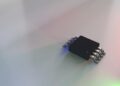
Representation of the TPS54331DR Buck Converter
The TPS54331DR, designed by Texas Instruments, is a 28-V, 3-A nonsynchronous buck converter with a low RDS(on) high-side MOSFET. This versatile power management solution is engineered for efficiency, featuring an Eco-mode for pulse skipping at light loads and an ultra-low 1-μA shutdown current, making it ideal for battery-powered applications.
With current mode control and internal slope compensation, the device simplifies external compensation design while reducing component requirements.
Key features include:
- input undervoltage lockout,
- overvoltage transient protection,
- and thermal shutdown
Together, these ensure robust performance under a variety of conditions. Packaged in a thermally optimized 8-pin SOIC, the TPS54331DR is a compact and reliable choice for efficient power conversion from 3.5V to 28V. The article below explores the specifications and design considerations detailed in the TPS54331DR datasheet.
TPS54331DR: PIN Configurations and Functions
The figures below present the PIN configurations of the TPS54331DR.
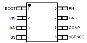
8-Pin SOIC D Package (Top View)
The pin configuration of the TPS54331DR is designed to optimize functionality and simplify circuit integration. The device features eight primary pins:
- The BOOT pin (1) requires a 0.1-μF bootstrap capacitor between BOOT and PH, which ensures the high-side MOSFET operates correctly by refreshing the capacitor voltage.
- The VIN pin (2) accepts the input supply voltage in the range of 3.5 V to 28 V, making it versatile for various applications.
- The EN pin (3) serves as the enable/disable control, with a pull below 1.25 V disabling the device, and it also allows for programming of the undervoltage lockout (UVLO) threshold using a resistor divider.
- The SS pin (4) is used to set the output rise time through an external capacitor, facilitating control of the slow-start function.
- The VSENSE pin (5) acts as the inverting input of the transconductance error amplifier, crucial for feedback regulation.
- The COMP pin (6) is the error amplifier output and connects to frequency compensation components for stabilizing the control loop.
- The GND pin (7) serves as the ground connection, essential for proper circuit operation.
- The PH pin (8), which is the source of the high-side power MOSFET, is connected to the inductor and manages the switching operation.
TPS54331DR: Design Advice Regarding Functional Modes
As described in the TPS54331DR datasheet, the buck converter operates in distinct functional modes to optimize performance under varying conditions, ensuring high efficiency and operational reliability across a wide range of applications.
Eco-Mode
At light load currents, the TPS54331DR enters pulse-skipping Eco-mode to maximize efficiency. This mode:
- Activates when the peak inductor current falls below 160 mA (typical).
- Disables the high-side integrated MOSFET to reduce switching losses.
- Internally clamps the COMP pin voltage at 0.5 V.
The device exits Eco-mode when the peak inductor current rises above 160 mA, allowing the COMP pin voltage to increase beyond 0.5 V. It is important to note that the average load current at which Eco-mode activates can vary depending on the application and the configuration of external output filters. This feature is particularly beneficial in systems with frequent low-load conditions, such as battery-powered devices, as it extends battery life by reducing power consumption.
Operation with VIN Below 3.5 V
The TPS54331DR is designed to operate with input voltages above 3.5 V; however, the device can function down to the undervoltage lockout (UVLO) threshold, which is application-dependent. Below the UVLO threshold, the device halts switching activity to protect the circuitry. If the EN pin is externally pulled high or left floating, the device becomes active once the VIN voltage exceeds the UVLO threshold. Switching is initiated following the slow-start sequence, ensuring a controlled ramp-up of the output voltage. This operational mode ensures robust performance even in systems where transient dips in input voltage may occur.
Operation with EN Control
The enable (EN) pin offers precise control over the device’s operational state. When the EN pin voltage is held below the typical threshold of 1.25 V:
- the TPS54331DR remains disabled
- switching is inhibited regardless of the VIN voltage
- the device enters a low-power quiescent mode, reducing IC current consumption.
When the EN pin voltage exceeds the threshold and the VIN voltage is above the UVLO level, the device transitions to an active state, enabling switching and initiating the slow-start sequence. This flexibility in control simplifies power sequencing and allows designers to implement custom enable/disable schemes for their applications.
TPS54331DR: PCB Design
In addition to the characteristics above, the TPS54331DR datasheet provides more information for your PCB layout design. As shown in the schematic, footprint, and 3D model below, your component’s CAD model and data must be accurate and from a trusted database to be helpful.
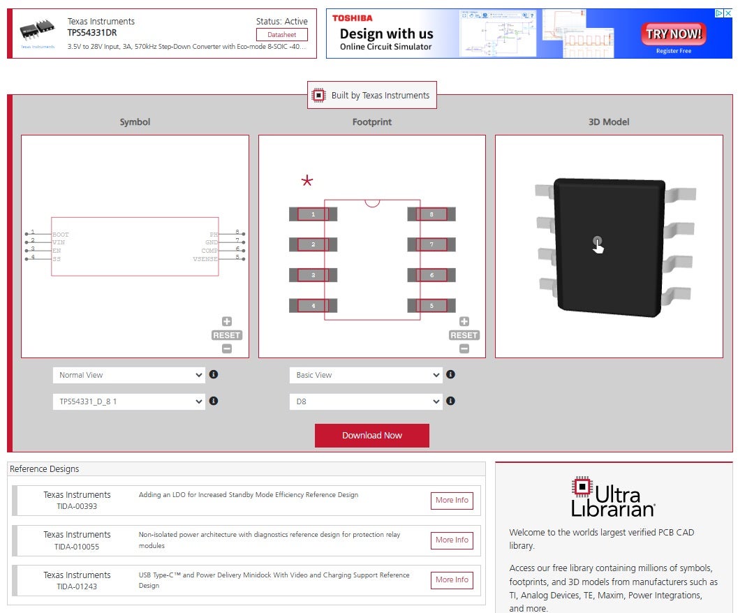
TPS54331DR schematic symbol, footprint, and 3D CAD model from UL
If you’re looking for CAD models for common components or more information on the TPS54331DR datasheet, Ultra Librarian helps by compiling all your sourcing and CAD information in one place.
Working with Ultra Librarian sets up your team for success to ensure streamlined and error-free design, production, and sourcing. Register today for free.


