
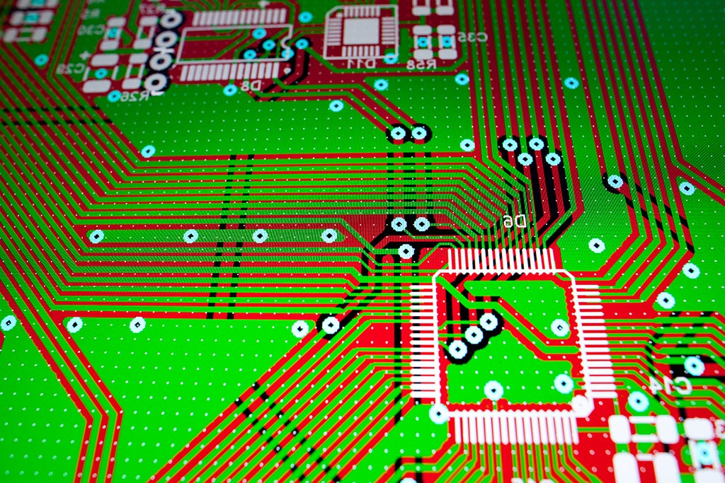
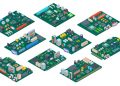
PCB component library creation ensures accuracy, efficiency, and consistency in the PCB design process. A PCB library allows engineers to define schematic symbols and PCB footprints based on component datasheets, reducing the possibility of design errors and manufacturing problems. With a well-organized library, engineers can reuse and verify components for future projects while staying in compliance with industry standards. In addition, shared libraries facilitate collaboration within teams by providing access to validated components for all members. PCB libraries improve design workflows, boost reliability, and support manufacturability, especially when working with unique components and complex designs.
The PCB Library Creation Process
Creating a PCB library is essential for producing reliable PCB designs, especially in complex or large-scale engineering projects. The following table provides an actionable overview for creating a robust and reusable PCB library.
PCB Footprint Creation Guidelines and Process
As noted above, creating PCB footprints is a key step in PCB library creation. Let’s take a closer look by examining two common methods of PCB footprint creation.
Manual Creation from Datasheets
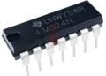
If you’ve been involved in the systems design process, you probably have datasheets available for your desired components. Many datasheets will include physical dimensions for PCB footprints and pin diagrams that can be used to create schematic symbols. The typical process for designing PCB footprints and schematic symbols from your datasheets is shown below.
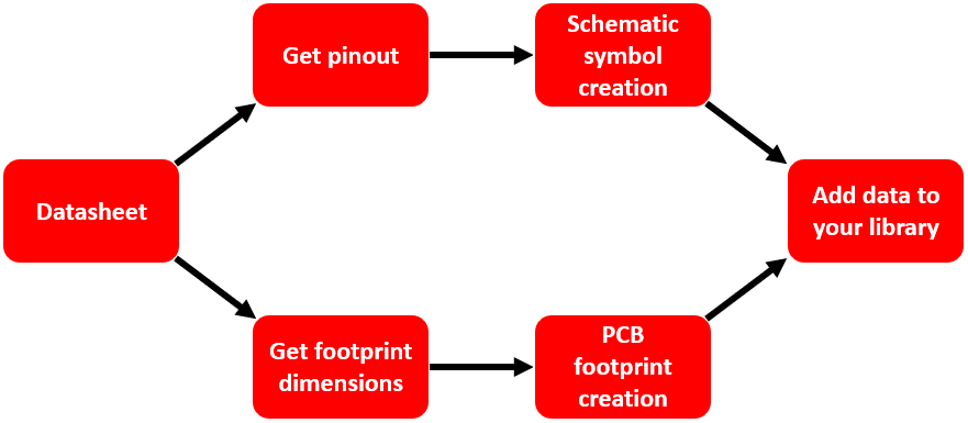
Manually creating component libraries can be difficult, and time consuming. More importantly, this method significantly increases the possibility of dimensional error that can cause several problems during assembly and operation. Mismatched pin-trace alignment, tombstoning and unpredictable performance are examples of possible failure modes.
Using Existing Library Parts
Using existing library part models is the preferred way to start your PCB footprint library. Many component footprints are standardized, so you can import existing footprints to a new component as long as the footprints match precisely. The required modifications might involve changing the component thickness in a 3D model or adding a ground pad (die-attached paddle) to the bottom of the component.
You would still have to create a new corresponding schematic symbol for the imported component. You’ll also need to access the datasheet and read through the pin diagram. Then, you would create the schematic symbol in your computer-aided design (CAD) software and export the part data to a component library. Either of these options can be useful for you and your design teams.
Saving Time During PCB Design
Because of the time involved in manual footprint creation, and the potential for mistakes, there are some third party “component wizard” applications you might consider. Also, high-quality CAD tools often include component creation wizards (including IPC-compliant footprint wizards). These tools are great for integrated circuit design. However, unique electronic components and mechanical parts will still need to be created or edited manually, taking time and effort away from more intensive processes like layout, routing, or verification.
PCB designers should focus on creating great new technology, rather than focusing on following PCB footprint creation guidelines. The time-consuming process for component creation is one reason “PCB Librarian” is still a common job title at many companies. Instead of manually creating and managing your component footprints, you can take advantage of a third party tool or service to acquire component footprints.
Ultra Librarian works with major component manufacturers and worldwide distributors to obtain verified PCB footprints and models. Rather than paying for a subscription to a component data supplier or scouring manufacturer websites for component data, you can access millions of verified components for free. You shouldn’t have to completely change your design simply because you can’t find a component model. Instead, you can instantly download part data and immediately import it into popular ECAD tools.
While footprint creation and manually creating design libraries can be optimized and done properly, in most settings, PCB library creation is easier to work from what’s already out there. Whether you need to find the component models and footprints you need now or set up your team for long-term success, Ultra Librarian is an easy and efficient way of procuring the information you need. Our Virtual Librarian Service (VLS) helps engineering teams create their own exclusive part libraries fast and accurately, allowing engineers to focus on innovation. Register today for free!

