
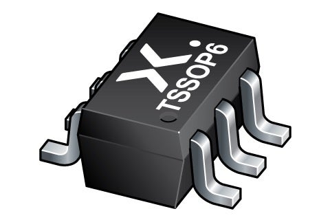
The NX3008NBKS datasheet has all the information necessary for circuit simulation and layout.
Without power, electronics don’t function. Power has become an increasingly important aspect of modern devices due to the constraints of onboard (i.e., battery-supplied) power, which enhances the device’s uptime between charges. Today, the MOSFET is the premier power component for general applications due to extremely low switching losses. The NX3008NBKS datasheet provides essential information for the component and some ideas for designers to leverage component capabilities.
The NX3008NBKS Datasheet Summary
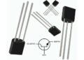
The NX3008NBKS is a dual n-channel MOSFET in an SMD-capable SOT363/SC-88 package for compact circuit placement and routing. The NX3008NKS utilizes trench MOSFET technology to provide more comprehensive vertical current flow (think vias connecting outer-layer power circuitry to an internal layer) for more efficient power consumption. Consider some of the benefits of the component mentioned in the NX3008NBKS datasheet:
- Very fast-switching – The shape of the trenches – deep with rounded corners extending into the drift region of the drain – reduces the gate-to-drain capacitance that serves as a bottleneck for transition states. Therefore, a trench MOSFET significantly reduces transition times, enhancing applications for high-speed designs and reducing power losses during switching.
- Low threshold voltage – Provided significant energy, charge carriers can cross over the Si-SiO2 barrier and remain trapped between the gate dielectric. In this region, these hot charge carriers induce proportionally large voltage swings due to their potential and temperature stress, which change the material performance. The NX3008NBKS’ superior construction tamps down on the ability of charge carriers to cross into this region and undermine stable performance.
- AEC-Q101 qualified – AEC-Q101 is a stress-test-based failure mechanism for semiconductor components in automotive applications; the NX3008NBKS is ready to meet the needs of modern automotive architecture.
NX3008NBKS Applications
However, the automotive qualification doesn’t mean the NX3008NBKS is only suitable for automotive applications; designers can also realize the excellent performance of the component in more general circuit topologies:
- Relay driver – Designs using microcontrollers require a buffer between the control board and the relay, as the microcontroller is unlikely to be able to supply enough current alone to operate the relay, and the back-EMF from the relay switching could potentially damage the microcontroller’s sensitive pins. The NX3008NBKS, inserted between the microcontroller and the relay – amplifies the current signal sent from the microcontroller to an appropriate level and possesses a high input impedance to dissipate the back-EMF from the relay.
- Low-side loadswitch – A low-side loadswitch positions the MOSFET between the load and the ground. This setup uses n-channel MOSFETs and is the easiest design to implement, as the gate only has to switch on the supply rail.
- High-speed line driver – A line driver provides a buffer between the source and the load – the state of the signal (digital high/low) on the input is the same on the output. However, line drivers also amplify the signal’s strength to contend with any loss in signal strength over the traversal path and boost the current to account for multiple loads drawing from the same source.
- Switching circuits – With its low gate-to-drain capacitance, the NX3008NBKS makes excellent, low-power digital switches.
Ultra Librarian Simplifies Library Management
The NX3008NBKS datasheet provides all the pertinent information designers need to get started with their circuit simulation or layout. However, not all designers or design teams have the time to build SPICE models and land patterns for every component. Fortunately, Ultra Librarian has the answer: with millions of verified component CAD models, symbol, footprint or 3D model creation no longer has to hold back the design timeline. The best part? Users can get started with Ultra Librarian by registering for free.
Working with Ultra Librarian sets up your team for success to ensure streamlined and error-free design, production, and sourcing. Register today for free.

